
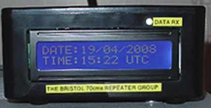
The Mark I GPS Clock (2008)
- Overview: Commissioned for the Bristol 70cm Repeater Group in 2008 as a proof-of-concept, the Mark I GPS Clock solved a critical timing drift issue on their active repeater infrastructure. By leveraging satellite-based GPS timestamps to automate hourly time synchronisation, it eliminated manual adjustments and laid the technical groundwork for our line of timing solutions.
Specification | Details |
Client / Scope | Bristol 70cm Repeater Group (Field Deployment) |
Core Architecture | Microchip PIC16C84 microcontroller |
Time Source | Trimble GPS Receiver (NMEA sentence parsing) |
User Interface | 16×2 LCD display, hardware DIP switches |
Primary Function | Automated UTC time correction for Arcom RC210 controllers |
Key Milestones & Legacy:
- Proven Field Reliability: Successfully deployed in an operational repeater environment, maintaining continuous synchronization without manual intervention.
- Firmware Foundation: Established a portable C-based firmware architecture that scaled into our subsequent product lines.
- Product Evolution: The operational feedback from this initial deployment directly drove the development of the commercial Mark II, III, and IV series.
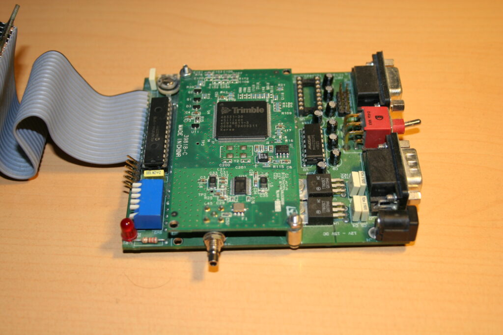
The Mark II GPS Clock (2010)
- Overview: Developed in 2010 as an upgraded architecture platform, the Mark II addresses the hardware constraints of the original prototype. Moving to an expanded microcontroller architecture provided increased memory and I/O capability, allowing for enhanced stability and refined firmware execution while maintaining full compatibility with Arcom RC210 controllers.
Specification | Details |
Primary Architecture | Microchip PIC16F877 microcontroller |
Hardware Design | Through-hole PCB layout (optimized for field repairability) |
Time Source | High-precision GPS module (NMEA 0183 protocol parsing) |
Deployment Strategy | Limited pilot evaluation / Internal reference architecture |
Primary Function | Scheduled pre-hour UTC time injection for repeater controllers |
Key Milestones & Engineering Insights:
- Scalable Microarchitecture: Successfully migrated the firmware framework to a higher-capacity platform, validating that the code base could scale for future feature integration.
- Serviceable Hardware Philosophy: Prioritized a robust, through-hole PCB design to support ease of maintenance and long-term serviceability in harsh field environments.
- Supply Chain Prudence: Faced with global component volatility and shifting module availability in 2010, production was strategically paused to avoid long-term delivery risks, prioritizing reliability over rushed commercial distribution.
- Bridging Innovation: Served as the crucial development link, directly informing the refined hardware architecture later commercialized in the Mark III and Mark IV series.
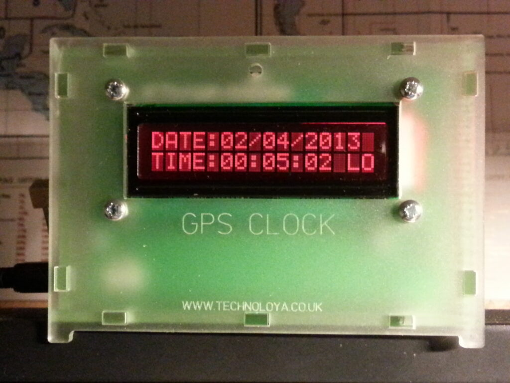
The Mark III GPS Clock (2013)
- Overview: Engineered in 2013 as our first compact, commercially packaged unit, the Mark III modernized the GPS Clock line by combining mature GPS technology with custom housing. Utilizing a streamlined PCB layout alongside an optimized enclosure design, it introduced international operational capabilities to expand beyond regional markets.
Specification | Details |
Core Processor | Microchip PIC16F877 microcontroller |
GPS Module | Integrated Trimble GPS clock board (NOS integration) |
Enclosure | Precision custom enclosure engineered by PCATs (Frome) |
User Interface | Compact 16×2 LCD display |
Localization | Expanded firmware supporting both UK and US Daylight Saving Time (DST) |
Key Milestones & Engineering Insights:
- Custom Enclosure Integration: Partnered with PCATs in Frome to engineer a dedicated, easy-to-assemble chassis, transitioning the product line from off-the-shelf project boxes to a purpose-built hardware platform.
- Global Compatibility: Upgraded core firmware to support multiple Daylight Saving Time protocols, expanding operational viability for North American and European repeater networks.
- Streamlined Footprint: Redesigned the main board geometry to optimize component density, resulting in a significantly reduced physical footprint and lower manufacturing unit costs.
- International Pilot Program: Distributed evaluation units across both UK and US markets, proving our ability to manufacture, package, and export functional hardware internationally.
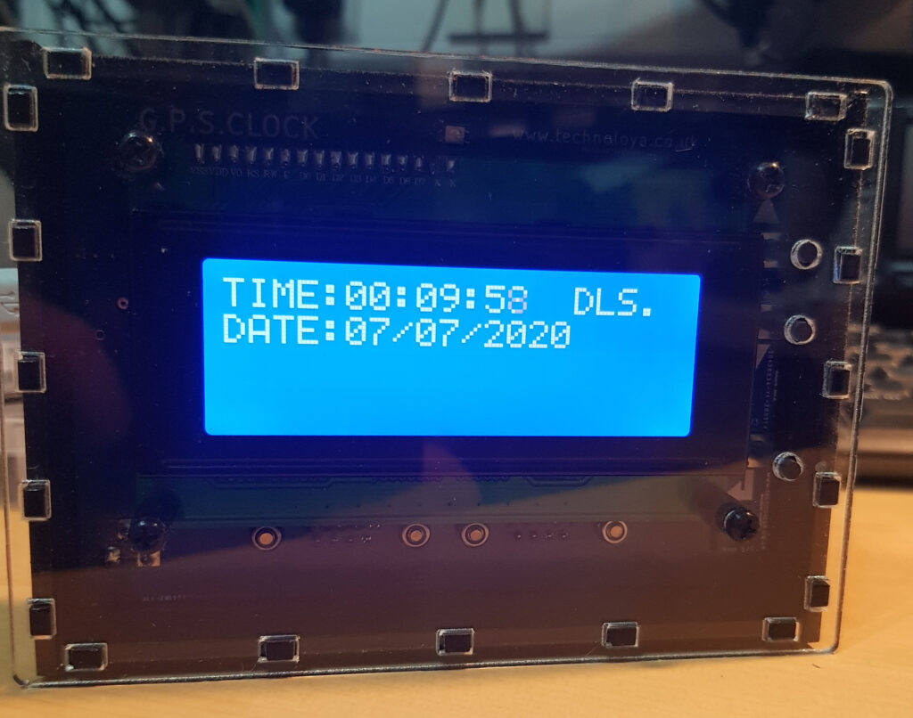
The Mark IV GPS Clock (2015)
- Overview: The Mark IV represented a complete architectural reinvention, shifting from legacy microcontrollers to a high-performance 32-bit platform. Featuring a full software UI, surface-mount manufacturing, and global timezone capabilities, the Mark IV became our first widely distributed commercial success across international markets.
Specification | Details |
Core Architecture | PJRC Teensy platform (ARM Cortex micro-architecture) |
GPS System | High-sensitivity u-Blox receiver (upgraded from EOL Trimble units) |
Manufacturing | Advanced hybrid Surface-Mount Technology (SMT) PCB layout |
User Interface | 4×20 character LCD display with 3-button navigation & NVRAM storage |
Enclosure | Custom PCATs housing (Gloss black body with clear acrylic faceplate) |
Global Compatibility | Support for UK, US, and Australian DST, plus custom 5-minute UTC offsets |
Key Milestones & Engineering Insights:
- 32-Bit Microarchitecture Pivot: Transitioned from legacy PIC chips to the PJRC Teensy platform, unlocking higher clock speeds, dedicated hardware UART/I²C buses, and vastly expanded flash memory.
- Modernized User Experience: Replaced manual DIP switches with an intuitive menu-driven software interface and introduced a pass-through serial diagnostic mode for seamless field maintenance.
- Field-Upgradable Infrastructure: Developed a streamlined bootloader setup, enabling end-users to perform fast, on-site firmware updates via downloadable binaries without hardware recalls.
- Supply Chain Resilience: Resolved GPS rollover limitations by transitioning to modular u-Blox architecture, ensuring long-term hardware availability and improved signal lock sensitivity.
- Global Commercial Success: Expanded beyond local UK groups to achieve international adoption, exporting operational units across North America, Mainland Europe, Asia-Pacific, and Australia.

The Mark V GPS Clock (In Active Development – 2026)
- Overview: Currently in development, the Mark V represents the most significant architectural evolution in the project’s history. Moving beyond dedicated repeater infrastructure, it transitions the GPS Clock into a portable, dual-mode timing and telemetry station engineered for both permanent shack installations and field operations.
Specification | Provisional Details |
Connectivity & Time | Multi-constellation GPS & 2.4 GHz Wi-Fi (NTP synchronization) |
Display & Navigation | High-contrast OLED panel with side-mounted rotary control |
Power Management | Internal rechargeable battery with universal USB-C charging |
Geospatial Telemetry | Maidenhead Locator, WAB Grid Square, Lat/Long, and Altitude |
Enclosure & Form Factor | Compact, field-ruggedized chassis with ambidextrous control orientation |
Legacy & Aux Support | Optional modular add-on for RC210 controllers (via GPS or NTP) |
Key Innovations & Development Focus:
- Hybrid Synchronization: Combines satellite GPS with Wi-Fi-based Network Time Protocol (NTP), allowing seamless operation indoors, in urban environments, or deep in the field.
- Operator-Centric Telemetry: Computes real-time Maidenhead grid locators, Worked All Britain (WAB) squares, and elevation metrics directly from satellite position data for portable operators.
- Ergonomic Rotary Interface: Replaces traditional push-buttons with a smooth, rolodex-style rotary menu system featuring configurable left/right-handed display orientation.
- Field-Ready Power Architecture: Integrates an internal battery with standardized USB-C charging to deliver weekend-long operation away from mains power.
- Expanded Utility Suite: Introduces integrated station alarms, customizable night-operation ambient lighting, and non-standard UTC/city-based automatic timezone tracking.
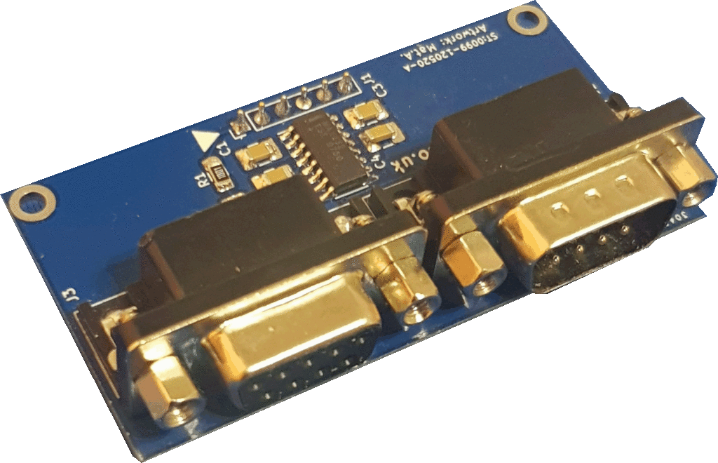
Twin RS-232 Interface Module (2020)
- Overview: Designed to streamline prototyping and embedded hardware testing, the Twin RS-232 Interface Module provides reliable, bi-directional serial level shifting in a compact form factor. Built around industry-standard driver architecture, it seamlessly bridges TTL/CMOS microcontroller logic with legacy or industrial RS-232 serial peripherals.
Specification | Details |
Core Transceiver | Maxim MAX3232 level-shifting IC |
Operating Voltage | 3.3 V to 5.5 V (Full 5 V logic tolerance) |
Signal Configuration | Dual-channel interface (1 x RS-232 Input / 1 x RS-232 Output) |
Form Factor | Breadboard-compatible pitch with standard jumper pin access |
Primary Application | Serial level translation, embedded prototyping, and hardware testing |
Key Capabilities & Application Value:
- Universal Microcontroller Compatibility: Wide supply voltage support allows direct, safe integration with both 3.3 V low-power ARM architecture and standard 5 V legacy microcontrollers.
- Prototyping-Optimized Layout: Form factor plugs directly into standard solderless breadboards, replacing bulky DB9 adapter cables with clean jumper-wire routing.
- Robust Signal Conditioning: Delivers stable, noise-tolerant voltage translation to ensure reliable serial data integrity across extended development cycles.
- Efficient Field Deployment: Minimizes hardware footprint while providing an immediate plug-and-play serial interface for embedded design validation.
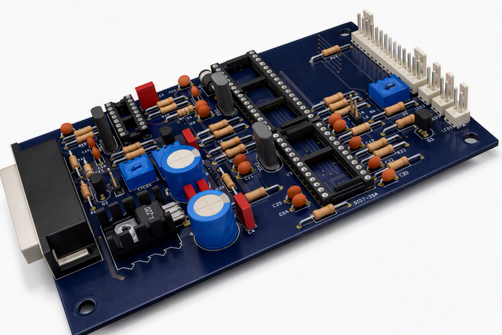
Custom Repeater Controller (Bespoke Engineering – 2021)
- Overview: Developed as a turn-key custom engineering project, this bespoke controller was built to exact client specifications, taking a customer-supplied schematic from concept to field-ready deployment. By combining precise PCB layout design with a tailored firmware architecture, the project delivered a robust, highly reliable hardware solution engineered for specialized repeater operations.
Specification | Details |
Core Architecture | Microchip PIC microcontroller (Custom firmware framework) |
Service Scope | Full-stack schematic translation, PCB layout design, and firmware delivery |
Design Validation | Custom 3D layout visual mock-ups and client review process |
Production Run | Short-run fabrication batch (5 boards engineered, 2 fully assembled/commissioned) |
Compliance & Data | Enterprise-grade GDPR compliance and client IP protection protocols |
Key Capabilities & Engineering Deliverables:
- Schematic-to-Production Engineering: Successfully converted raw customer schematics and functional requirements into an optimized, professionally routed printed circuit board.
- Deterministic Firmware Architecture: Implemented a clean, maintainable software framework to guarantee predictable timing behavior and rock-solid operational stability.
- Rapid Prototype Iteration: Provided detailed visual mock-ups prior to fabrication, enabling efficient customer feedback loops and design sign-offs.
- Flexible Short-Run Manufacturing: Accommodated specialized low-volume production requirements, ensuring cost-effective fabrication while supplying long-term hardware spares.
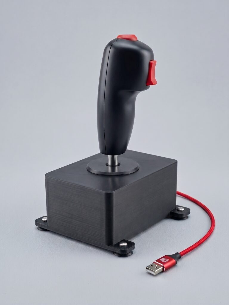
Adaptive USB Joystick Interface (Assistive Gaming Technology, 2021)
- Overview: Commissioned to restore accessibility for a PC gamer living with Multiple Sclerosis, this project integrated an industrial 8-way joystick with custom microcontroller interface hardware. By mapping physical joystick directional inputs to emulated keyboard controls (WASD), the custom solution restored full vehicle movement control in complex gaming environments. This project was completed and delivered to the client as a fully donated pro bono solution.
Specification | Details |
Core Architecture | PJRC Teensy LC (Human Interface Device / HID Keyboard Emulation) |
Input Hardware | Industrial 8-sector heavy-duty joystick |
Enclosure | Custom 3D-printed modular chassis (Interlocking, fastener-free design) |
Mounting System | Integrated suction-base array for high-stability desk adhesion |
Project Type | Fully donated assistive technology integration |
Key Capabilities & Engineering Deliverables:
- Custom HID Control Emulation: Configured low-latency firmware to translate industrial switch closures into standard USB keyboard keystrokes, eliminating the need for complex dexterity on traditional keyboards.
- Fastener-Free Modular Chassis: Designed a toolless, 3D-printed interlocking enclosure that simplified assembly while maintaining full field-serviceability.
- Ergonomic & High-Stability Mounting: Integrated surface-suction mounting geometry directly into the base layout, securing the controller during intense operational use without desk drift.
- Rapid Prototyping & Financial Aid: Rapidly moved from requirements gathering to functional hardware, providing the entire solution (engineering, materials, and final product) at no financial cost to the client.
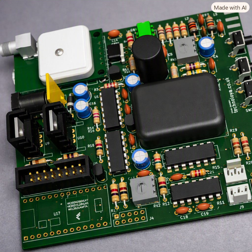
GPS-Disciplined OCXO (Precision Frequency Reference – 2021)
- Overview: Engineered to deliver ultra-stable, long-term frequency accuracy, this GPS-disciplined Oven-Controlled Crystal Oscillator (OCXO) bridges precision satellite timing with high-stability oscillator hardware. Manufactured to strict client specifications, the project involved translating a complex RF/timing schematic into a production-ready PCB tailored to fit a pre-selected enclosure.
Specification | Details |
Technology Class | GPS-Disciplined Oven-Controlled Crystal Oscillator (GPSDO) |
Service Scope | Full schematic-to-PCB translation, enclosure-constrained layout, & prototyping |
Design Validation | Detailed 3D CAD modeling and enclosure-fit visual mock-ups |
Production Run | Low-volume prototype fabrication (5-board production batch) |
Data Security | Enterprise-grade confidentiality and GDPR-compliant IP management |
Key Capabilities & Engineering Deliverables:
- Precision RF/Timing PCB Design: Precision-routed printed circuit board layout designed to maintain signal integrity and thermal stability for high-precision OCXO hardware.
- Enclosure-Constrained Mechanical Fitting: Engineered the board footprint to meet strict physical dimensional constraints, ensuring seamless integration into the client’s chosen chassis.
- Collaborative Design Optimization: Provided critical layout refinements and structural suggestions during the 3D mock-up phase, ensuring smooth client sign-off prior to manufacturing.
- Turn-Key Manufacturing Support: Managed short-run PCB fabrication, delivering primary operational units alongside long-term hardware spares.
Radio Transceiver Control System & Front Panel PCB (2025)
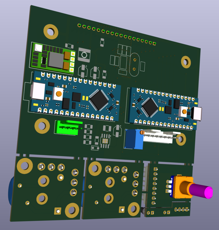
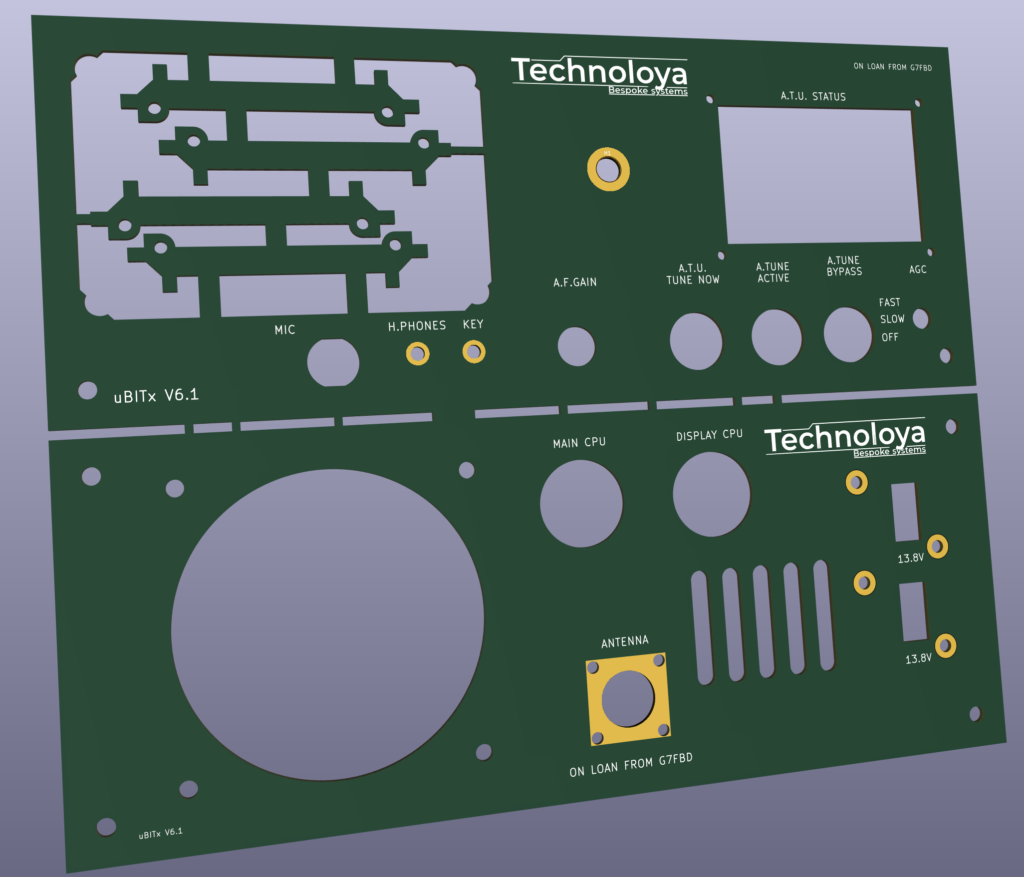
Overview: Commissioned in 2025, this project required designing a custom PCB control architecture and integrated front panel layout for a radio transceiver system. The solution features a dual-processor architecture to segregate system management from display processing, along with a custom PCB front panel engineered with specialized ground plane isolation and plated through-hole grounding.
| Specification | Details |
| System Architecture | Dual Microcontroller Layout (Main CPU & Dedicated Display CPU) |
| Application | HF Radio Transceiver Platform |
| Front Panel PCB | PCB-fabricated front enclosure panels with custom silkscreen labeling |
| RF & Shielding Design | Full rear-side ground plane with selective plated through-hole grounding |
| Integrated Controls | ATU control suite, AGC response selection, AF gain, and DC power distribution |
Key Capabilities & Engineering Deliverables:
Dual-Processor Core Integration: Split main system logic and UI rendering across two onboard microcontrollers (Main CPU and Display CPU), ensuring responsive control during active tuning and transmission.
RF Shielding & Ground Plane Engineering: Designed the front panel PCB with a full rear ground plane and exposed grounding points around key chassis holes, utilizing plated through-holes to minimize RF noise coupling into front-panel controls.
Custom Enclosure Panel Fabrication: Engineered structural PCB panels featuring mouse-bite breakaways, precision cutouts for displays and meters, and custom silkscreen legends for clean, professional front-panel assembly.
Turn-Key Controls Routing: Integrated onboard mounting for rotary encoders, audio gain potentiometers, ATU status indicators, and DC power connectivity directly onto the control system board, minimizing point-to-point wiring complexity.